Skip to content

Teach Semiconductor Electronics: Materials, Devices and Simple Circuits in eight steps.

For each idea: show it, ask before you tell, then say one line.

Gather paper and a pencil.

Common misconceptions & worked visual for this chapter · 15 practice questions with answers

How to teach it

Materials and charge carriers

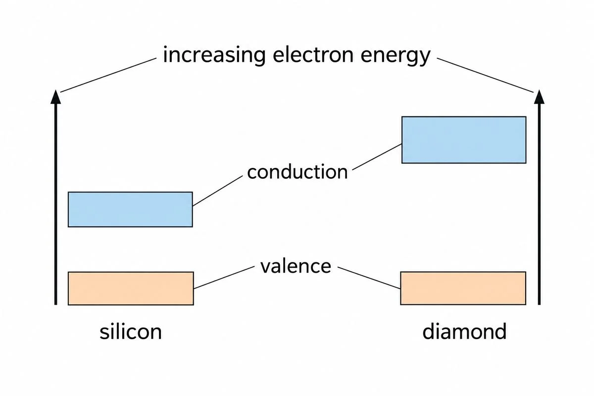
Diagram comparing silicon’s smaller energy gap with diamond’s larger gap.

1. Energy bands

Bands describe allowed electron energies within a solid.

Show
Find silicon’s valence and conduction bands in the diagram. Compare its gap with diamond’s. Follow the arrow showing increasing electron energy.
Ask
Which gap would an electron need more energy to cross?
Say
In pure crystals, electrons have allowed energies within the bands, but none within the gaps. Crossing diamond’s larger gap needs more energy.
Used in
Large band gaps help wire insulation reduce unwanted current.
If your child says…“Equal outer-electron counts mean equal gaps.”
Ask
Does counting outer electrons tell us how strongly atoms bond?
What’s true
Diamond and silicon have matching outer-electron counts but different gaps.
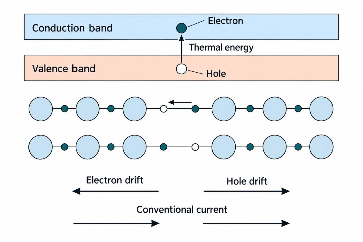
Electron–hole creation, vacancy movement and opposite drifts producing conventional current in the same direction.

2. Electrons and holes

Electrons and positive holes both carry current.

Show
Find the heat-freed electron in the diagram. Follow the bond electron filling a hole below. Compare the drift and conventional-current arrows.
Ask
Where will the hole move when the neighbouring electron fills it?
Say
The hole shifts to the electron’s previous place and behaves positively. Their opposite charges make both conventional currents point the same way.
Used in
Sunlight creates electron–hole pairs in solar cells, producing electricity.
If your child says…“A hole is another negative electron.”
Ask
Does the empty bond position contain an extra electron, or lack one?
What’s true
A hole is an electron vacancy that behaves positively.
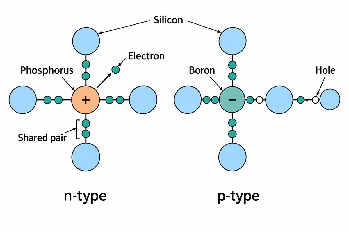
Phosphorus supplies an extra electron; boron leaves a vacancy in silicon bonds.

3. Doping

Added impurities make electrons or holes the majority carriers.

Show
Find phosphorus and boron in the diagram. Follow phosphorus’s extra electron and boron’s moving vacancy.
Ask
Which mobile carrier would each replacement atom add to silicon?
Say
Phosphorus adds a mobile electron; boron creates a hole.
Used in
Doping forms regions in electronic switches, allowing circuits to control current.
If your child says…“An n-type crystal is negatively charged.”
Ask
Does freeing an electron remove the positive charge balancing it?
What’s true
Fixed dopant ions balance carrier charges, keeping the bulk neutral.

The junction and diode

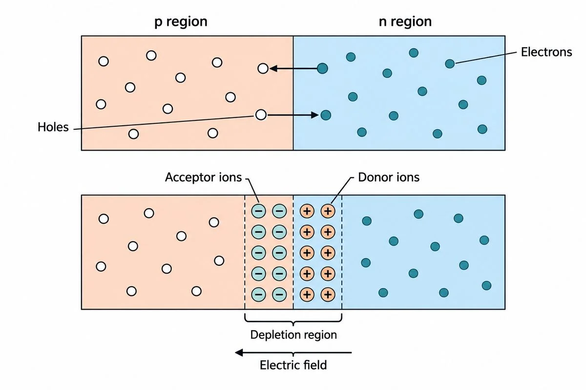
Carrier diffusion leaves fixed junction ions and an electric field pointing from n to p.

4. The p–n junction

Diffusion leaves ions whose field opposes further carrier spreading.

Show
Follow electrons and holes across the diagram’s upper junction. Find the fixed ions below. Trace their electric field from n to p.
Ask
How will this growing junction field affect further majority-carrier diffusion?
Say
Carriers spread and recombine, leaving fixed charged ions near the junction. These ions create an electric field opposing further majority-carrier diffusion.
Used in
Light-sensing junctions turn light into electrical signals.
If your child says…“The depletion region has no charge.”
Ask
What creates the field if the depletion region has no charge?
What’s true
The region loses mobile carriers, but fixed charged ions remain.
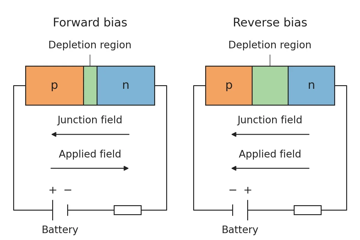
Opposite battery connections produce narrow forward-bias depletion and wider reverse-bias depletion.

5. Forward and reverse bias

Supply polarity changes depletion width.

Show
Trace each battery’s positive connection in the diagram. Compare the applied-field and junction-field arrows. Then compare the depletion widths.
Ask
How will reversing this battery change the depletion width and current?
Say
Forward bias lowers the barrier and narrows depletion. Reversing the battery raises the barrier and widens depletion. Below breakdown, minority carriers still carry a small reverse current.
Used in
Rectifiers use changing bias to select when a diode conducts.
If your child says…“Connecting p to positive gives reverse bias.”
Ask
Which connection lowers the barrier?
What’s true
Forward bias puts p at a higher potential than n.

VR=VS−VDV_R=V_S-V_D

VR=5.0−0.7=4.3 VV_R=5.0-0.7=4.3\,\mathrm{V}

6. Diode circuit models

A stated diode drop leaves less voltage for the resistor.

Show
Write these lines. Name resistor, supply and diode voltages VRV_R, VSV_S and VDV_D. Use 5 V, a 1 kΩ series resistor and an assumed 0.7 V forward drop. The diode’s anode faces supply positive.
Ask
What current flows through the resistor and diode?
Say
The current is 4.3 mA. Divide the resistor’s remaining voltage by its resistance.
Used in
An external resistor limits diode current, helping prevent damage.
If your child says…“The resistor gets the whole supply voltage.”
Ask
After the diode’s voltage drop, can the resistor still have the whole supply voltage?
What’s true
The diode and resistor share the supply voltage.

Rectifying and smoothing

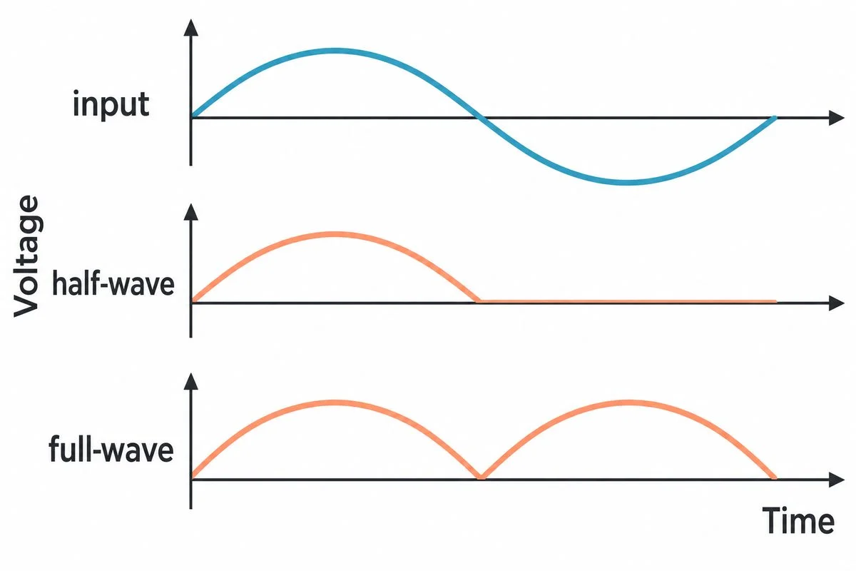
Three aligned traces show input, half-wave output and full-wave output.

7. Half-wave and full-wave rectification

Rectifiers produce current flowing one way.

Show
Find one complete input cycle in the diagram. Compare the half-wave and full-wave pulses within that interval.
Ask
How many full-wave pulses will the next cycle produce?
Say
Each cycle gives one half-wave pulse or two full-wave pulses. Neither output reverses current.
Used in
Rectifiers give chargers current flowing one way.
If your child says…“Full-wave output gives one pulse per cycle.”
Ask
How many upward humps fit beneath one complete input cycle?
What’s true
Full-wave output gives two pulses per input cycle.
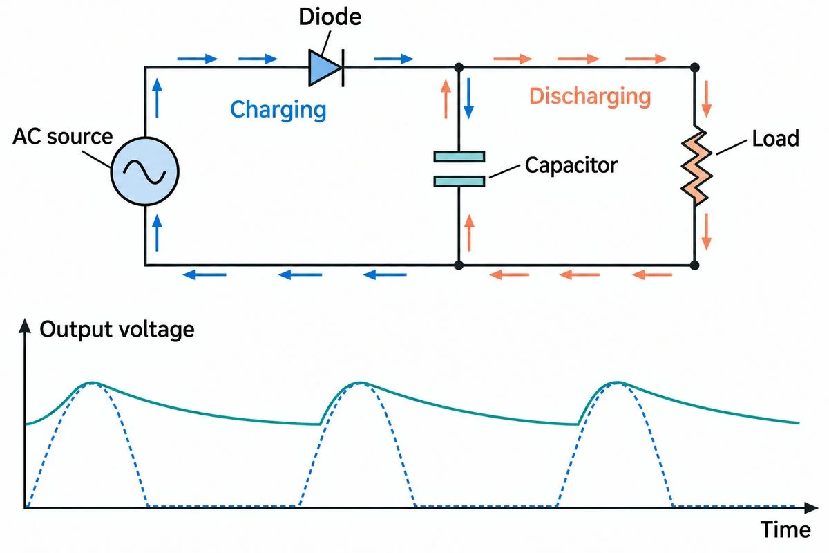
A parallel capacitor supplies the load between peaks, reducing the output voltage ripple.

8. Capacitor filtering

Stored charge supplies the load between rectified voltage peaks.

Show
Find the capacitor across the load in the diagram. Follow its charging and discharging paths. Compare the voltage traces between peaks.
Ask
What can supply the load while the diode is not conducting?
Say
The capacitor charges near each peak. Between charging intervals, the diode blocks and the capacitor supplies the load. Its voltage falls as it discharges, so filtering reduces ripple without removing it completely.
Used in
Capacitor filters reduce output voltage changes, giving the load a steadier supply.
If your child says…“The smoothing capacitor goes in series.”
Ask
Would that series connection keep supplying steady direct current?
What’s true
A series capacitor cannot pass steady direct current.

A real problem

The practical silicon solar cell addressed a remote telephone power problem.

Batteries deteriorated quickly in humid locations, so remote telephone systems needed another power source.

Researchers demonstrated the first practical silicon solar cell in 1954.

Absorbed sunlight creates electron–hole pairs in semiconductors, enabling solar cells to produce electricity.

American Physical SocietyU.S. Department of Energy

An unbranded solar panel on a rooftop in sunlight.

Concept Lab · Common misconception

The tempting mistake in Semiconductor Electronics: Materials, Devices and Simple Circuits

Open standalone misconception page →

Does a diode conduct as soon as any positive voltage appears?

Wrong

A silicon diode behaves like a short circuit at any forward voltage.

Why it feels right. The circuit symbol suggests a simple one-way switch.

Right

Real forward current grows strongly with forward voltage. The ideal switch is an approximation.

Worked example

This qualitative current–voltage curve shows very small current at low forward bias and much larger current near 0.7 V.
  1. Compare a typical silicon diode near 0.1 V and near 0.7 V forward bias.
  2. The current can be negligible in the first case and appreciable in the second, depending on the diode and circuit.

Ask your child eight quick questions.

One per step. The answer and the reason are given.

  1. How do diamond’s and silicon’s energy gaps compare?

    Diamond’s gap is larger. Their bonding differs despite matching outer-electron counts.

  2. What sign of charge does a hole behave as having?

    Positive. A missing negative electron leaves a vacancy that behaves as a positive charge.

  3. What is the whole crystal’s net charge after donor atoms release electrons?

    Zero. The positive donor ions balance the released electrons’ negative charge.

  4. What charged objects remain fixed inside the depletion region?

    Donor and acceptor ions. Depletion removes mobile carriers, leaving charged ions in the crystal.

  5. With p positive and n negative, what type of bias does the junction have?

    Forward bias. The p side is at a higher potential than the n side.

  6. The resistor needs 2.0 V and the diode takes 0.7 V. What supply voltage is needed?

    2.7 V. The supply must provide both voltage drops.

  7. A full-wave rectifier receives 50 input cycles each second. How many output pulses occur each second?

    100 pulses. Each input cycle contributes two output pulses.

  8. Where should the smoothing capacitor connect relative to the load?

    In parallel. Across the load, it supplies current between charging peaks.

15 more questions with answers, 2 with pictures